Introduction to LTCC (Low Temperature Co fired Ceramics) Technology

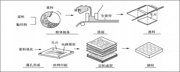
Low temperature co fired multilayer ceramics (LTCC, An integrated ceramic component is formed by sintering in a parallel printing coating process.
Our LTCC products have covered (filters, composite substrates, LED ceramic substrates, microwave transceiver modules, hybrid LTCC circuits, 3D-MCM modules, etc.). At present, the company's production capacity is about 1.5 million pieces/month for large-sized component substrates and 10 million pieces/month for small-sized component substrates. In addition, the capacity can be rapidly improved by increasing equipment and personnel according to user needs.
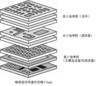
Low temperature co fired ceramic (LTCC) structure
Our company is committed to the localization of LTCC raw materials (raw ceramic tape, slurry) and cost reduction process (all silver plating, etc.), which can make the LTCC substrate price reach the level of traditional PCB, and is a process path suitable for products in the civil communication field.
The application frequency band of our LTCC ceramic substrate products can cover microwave low frequency to Ka band, and the number of layers reaches 40, aiming to provide customers with high-performance and reliable LTCC substrate customization services, LTCC passive components, integrated packaging components (SIP) and product miniaturization technology solutions.
Sample display:

characteristic:
LTCC process uses laser drilling, micro hole grouting, precision conductor slurry printing and other processes to produce the required circuit graphics on the raw ceramic belt, and embeds multiple passive components (such as low capacitance capacitors, resistors, filters, impedance converters, couplers, etc.) in the multilayer ceramic substrate, and then stacks them together. The inner and outer electrodes can be respectively made of silver, copper, gold and other metals, sintered at 900 ℃, It can be made into 3D space non-interference high-density circuit, or 3D circuit substrate with built-in passive components. IC and active components can be mounted on its surface to make passive/active integrated functional modules, which can further miniaturize and high-density circuits, especially suitable for high-frequency communication components.
Hotline
Scan WeChat
